- 您现在的位置:买卖IC网 > Sheet目录3855 > PIC16C62B-20/SS (Microchip Technology)IC MCU OTP 2KX14 PWM 28SSOP
PIC16C62B/72A
1999 Microchip Technology Inc.
Preliminary
DS35008B-page 51
When the A/D conversion is complete, the result is
loaded into the ADRES register, the GO/DONE bit,
ADCON0<2>, is cleared, and the A/D interrupt flag bit,
ADIF, is set. The block diagram of the A/D module is
shown in Figure 9-1.
The value that is in the ADRES register is not modified
for a Power-on Reset. The ADRES register will contain
unknown data after a Power-on Reset.
After the A/D module has been configured as desired,
the selected channel must be acquired before the con-
version is started. The analog input channels must
have their corresponding TRIS bits selected as an
input. To determine acquisition time, see Section 9.1.
After this acquisition time has elapsed, the A/D conver-
sion can be started. The following steps should be fol-
lowed for doing an A/D conversion:
1.
Configure the A/D module:
Configure analog pins / voltage reference /
and digital I/O (ADCON1)
Select A/D input channel (ADCON0)
Select A/D conversion clock (ADCON0)
Turn on A/D module (ADCON0)
2.
Configure A/D interrupt (if desired):
Clear ADIF bit
Set ADIE bit
Set GIE bit
3.
Wait the required acquisition time.
4.
Start conversion:
Set GO/DONE bit (ADCON0)
5.
Wait for A/D conversion to complete, by either:
Polling for the GO/DONE bit to be cleared
OR
Waiting for the A/D interrupt
6.
Read A/D Result register (ADRES), clear bit
ADIF if required.
7.
For next conversion, go to step 1 or step 2 as
required. The A/D conversion time per bit is
defined as TAD. A minimum wait of 2TAD is
required before next acquisition starts.
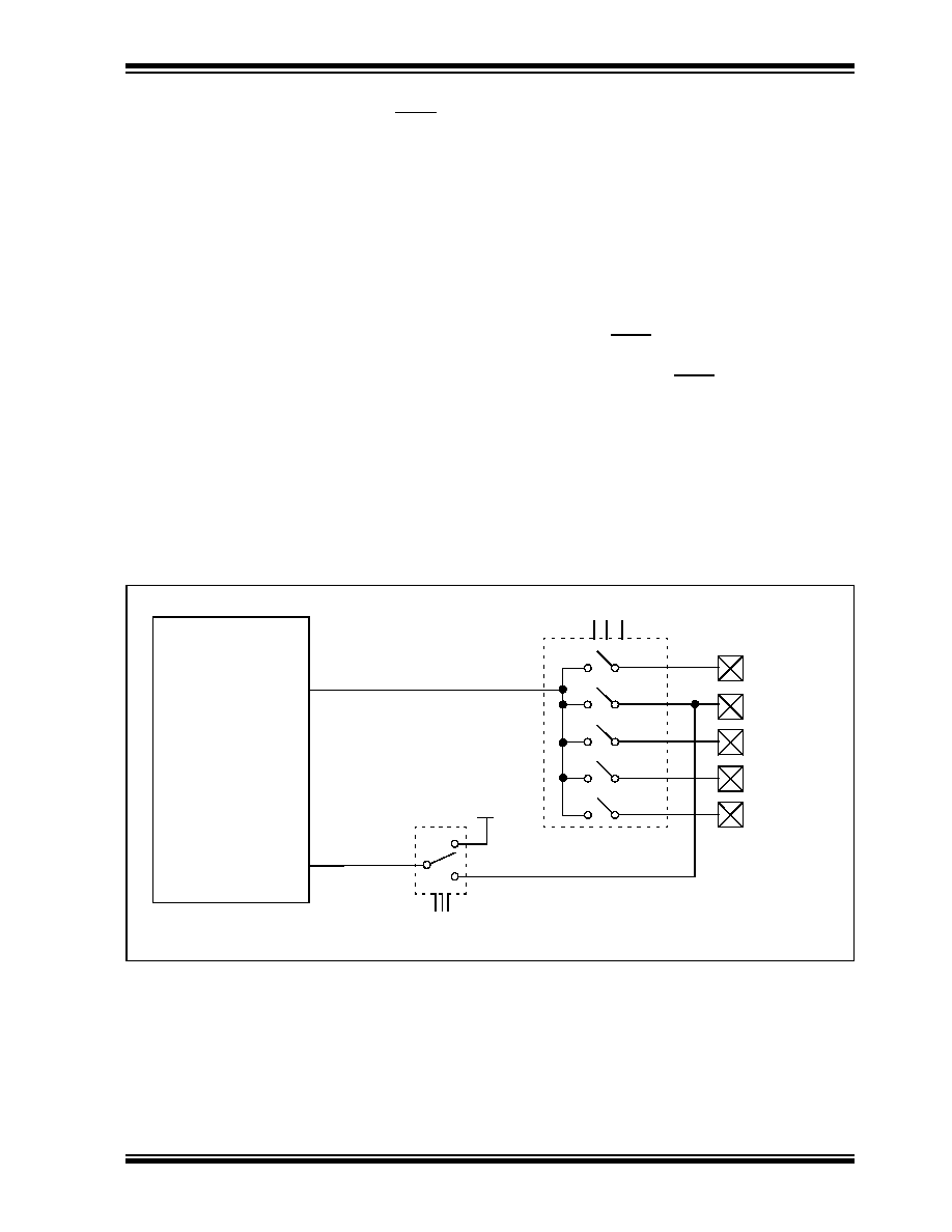
FIGURE 9-1:
A/D BLOCK DIAGRAM
(Input voltage)
VIN
VREF
(Reference
voltage)
VDD
PCFG2:PCFG0
CHS2:CHS0
000 or
010 or
100 or
001 or
011 or
101
RA5/AN4
RA3/AN3/VREF
RA2/AN2
RA1/AN1
RA0/AN0
100
011
010
001
000
A/D
Converter
11x
发布紧急采购,3分钟左右您将得到回复。
相关PDF资料
PIC16LC711-04I/SO
IC MCU OTP 1KX14 A/D 18SOIC
PIC18F66J90-I/PT
IC PIC MCU FLASH 64KB 64-TQFP
ATMEGA32L-8AC
IC AVR MCU 32K LV 8MHZ COM44TQFP
DSPIC30F2012-30I/SP
IC DSPIC MCU/DSP 12K 28DIP
PIC18LF2321-I/ML
IC PIC MCU FLASH 4KX16 28QFN
PIC18F4321-I/P
IC PIC MCU FLASH 4KX16 40DIP
ATMEGA32L-8MC
IC AVR MCU 32K LV 8MHZ COM 44QFN
PIC18F2450-I/SP
IC PIC MCU FLASH 8KX16 28DIP
相关代理商/技术参数
PIC16C62B-20E/SO
功能描述:8位微控制器 -MCU 3.5KB 128 RAM 22 I/O RoHS:否 制造商:Silicon Labs 核心:8051 处理器系列:C8051F39x 数据总线宽度:8 bit 最大时钟频率:50 MHz 程序存储器大小:16 KB 数据 RAM 大小:1 KB 片上 ADC:Yes 工作电源电压:1.8 V to 3.6 V 工作温度范围:- 40 C to + 105 C 封装 / 箱体:QFN-20 安装风格:SMD/SMT
PIC16C62B-20E/SP
功能描述:8位微控制器 -MCU 3.5KB 128 RAM 22 I/O RoHS:否 制造商:Silicon Labs 核心:8051 处理器系列:C8051F39x 数据总线宽度:8 bit 最大时钟频率:50 MHz 程序存储器大小:16 KB 数据 RAM 大小:1 KB 片上 ADC:Yes 工作电源电压:1.8 V to 3.6 V 工作温度范围:- 40 C to + 105 C 封装 / 箱体:QFN-20 安装风格:SMD/SMT
PIC16C62B-20E/SS
功能描述:8位微控制器 -MCU 3.5KB 128 RAM 22 I/O RoHS:否 制造商:Silicon Labs 核心:8051 处理器系列:C8051F39x 数据总线宽度:8 bit 最大时钟频率:50 MHz 程序存储器大小:16 KB 数据 RAM 大小:1 KB 片上 ADC:Yes 工作电源电压:1.8 V to 3.6 V 工作温度范围:- 40 C to + 105 C 封装 / 箱体:QFN-20 安装风格:SMD/SMT
PIC16C62B-20I/ML
功能描述:8位微控制器 -MCU 3.5KB 128 RAM 22 I/O RoHS:否 制造商:Silicon Labs 核心:8051 处理器系列:C8051F39x 数据总线宽度:8 bit 最大时钟频率:50 MHz 程序存储器大小:16 KB 数据 RAM 大小:1 KB 片上 ADC:Yes 工作电源电压:1.8 V to 3.6 V 工作温度范围:- 40 C to + 105 C 封装 / 箱体:QFN-20 安装风格:SMD/SMT
PIC16C62B-20I/SO
功能描述:8位微控制器 -MCU 3.5KB 128 RAM 22 I/O RoHS:否 制造商:Silicon Labs 核心:8051 处理器系列:C8051F39x 数据总线宽度:8 bit 最大时钟频率:50 MHz 程序存储器大小:16 KB 数据 RAM 大小:1 KB 片上 ADC:Yes 工作电源电压:1.8 V to 3.6 V 工作温度范围:- 40 C to + 105 C 封装 / 箱体:QFN-20 安装风格:SMD/SMT
PIC16C62B-20I/SO
制造商:Microchip Technology Inc 功能描述:8BIT CMOS MCU SMD 16C62 SOIC28
PIC16C62B-20I/SP
功能描述:8位微控制器 -MCU 3.5KB 128 RAM 22 I/O RoHS:否 制造商:Silicon Labs 核心:8051 处理器系列:C8051F39x 数据总线宽度:8 bit 最大时钟频率:50 MHz 程序存储器大小:16 KB 数据 RAM 大小:1 KB 片上 ADC:Yes 工作电源电压:1.8 V to 3.6 V 工作温度范围:- 40 C to + 105 C 封装 / 箱体:QFN-20 安装风格:SMD/SMT
PIC16C62B-20I/SP
制造商:Microchip Technology Inc 功能描述:IC 8BIT CMOS MCU 16C62 SDIL28